|
Chip
Wafer etched
with Switches and circuitry.
Acronym:
Ch = Wew-Sac (pronounced WUU-sak).
The theme is switches. And although switch technology has evolved over the
decades from hand-operated toggle switches, to electromagnetic switches, to
vacuum tubes, to transistors, in each case we're talking about using switches to
receive and send messages.
Chips are fingernail-sized wafers of layered semiconductor materials etched
with millions of
microscopic switches and circuitry. They hold
your data and instructions in the form of off/on patterns represented by 0s or
1s. Because a chip's surface combines, or
integrates,
various electronic components into one unit, chips are sometimes called
integrated circuits or ICs.
|
|
Max. If a chip is only the size
of my fingernail, how can it hold
millions of switches?
|
I'm amazed
myself, B.P. Here's a simplified
description of how chips are made.
|
| Making
Chips
Most chips are made of silicon
(SIL-ih-kawn), a natural
semiconductor and one of the most
abundant substances on earth. In
fact, silicon is the primary
component of beach sand. Trap:
Avoid embarrassment, do NOT
pronounce it silicone (SIL-ih-kohn),
which is a totally different
substance!
Semiconductors, unlike true
conductors, reluctantly transmit
electricity and can be switched
Off and On with a remotely-sent
electrical charge.
To start the chip-making
process, grains of silicon are
melted in high temperature
furnaces and shaped into
cylindrical ingots. After cooling,
the ingots are sliced into thin
circular wafers using a
diamond-bladed saw. These wafers
look metallic but are actually
brittle and delicate, like glass.
Once polished they shine like
silvered mirrors.
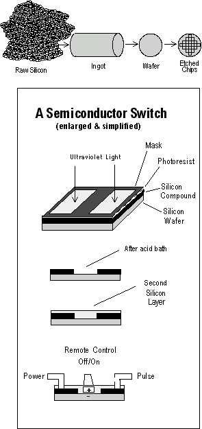
The switches and circuitry for
the chip start as several layers
of hand- or computer-drawn lines
and shapes which are optically
reduced to a microscopic fraction
of their original size. A
"mask" is then created
for each layer of circuitry.
The pure silicon wafer is
coated with a silicon compound and
a light-resistant material called photoresist.
The first mask is attached and the
assembly is exposed to ultraviolet
light. Where light passes through
the mask, it hardens the
photoresist. The exposed wafer is
then bathed in acid which eats
away the nonhardened photoresist
and etches the first layer of
circuitry into the silicon
compound.
|
 |
After
being recoated with more silicon
compound, photoresist, and the
second-layer mask, the wafer is
re-exposed to ultraviolet light
and another acid bath which etches
the second layer of circuitry.
This process is repeated perhaps
dozens of times until all layers
of circuitry are etched into the
wafer.A single wafer typically holds
hundreds of chips which are then
cut into individual pieces. |
Protective Housing
Although chips appear to be metallic,
they are more like glass in character, hence very brittle. For protection,
each chip is mounted inside a plastic or ceramic housing. This housing
looks like a square or rectangular bug with several metal legs sticking
out. Tiny wires attach the chip's circuits to the metal pins. These pins
then plug into the computer's circuit boards, putting the chip into
contact with the rest of the computer. |

|
|
The three major chip types are CPU, RAM, and
ROM, and we'll cover each of these separately.
|
Click here to return to the top of this page
|